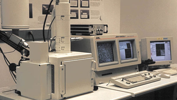
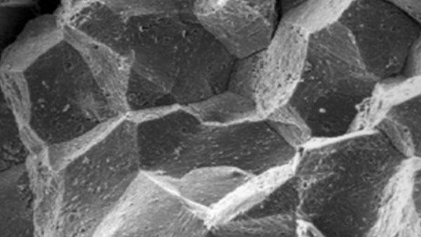
Scanning electron microscopy (SEM) analyzes the surface of materials. SEM measures and evaluates surface pitting, failure analysis, characterization of dust, deposits, contaminants, particles, filter residues, and other applications.
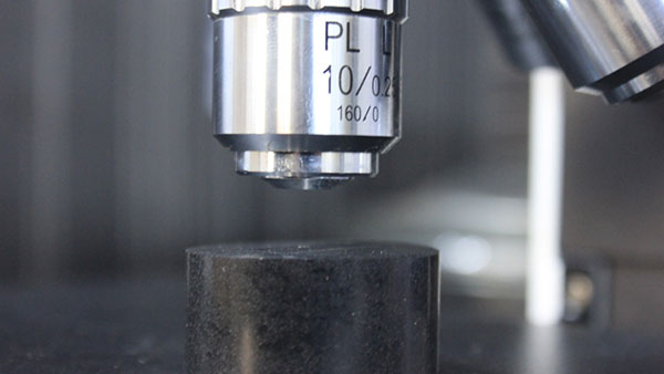
MTS Metallurgists analyse the surface of solid objects, producing higher resolution images than optical microscopy. Micro structural characterization includes the analysis of materials, polymers, films, coatings, geological and mineral core samples, pharmaceuticals, raw materials, metals, plastics, ceramics, glass, food, dust, contaminants, unknowns and other products.
MTS reviews the data produced by SEM labs provide elemental analysis of solid samples, impurities, and the identification of physical and chemical defects. The laboratories provide analytical surface science expertise to support research, failure analysis, troubleshooting, quality control and other requirements.
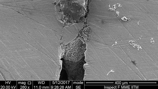
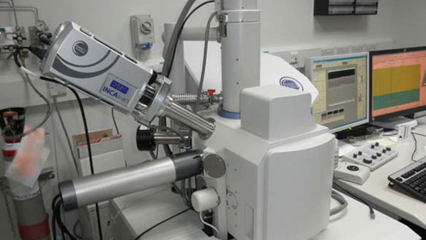
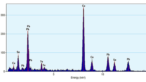
SEM/Energy Dispersive X-ray Analysis is also available. SEM/EDXA allows the analysis of small particles by scanning electron microscopy and energy dispersive X-ray analysis, resulting in testing without destruction or injury to the sample. SEM/EDXA provides qualitative elemental analysis and element localization on samples being analysed. MTS has a tie up with leading SEM service providers in India and abroad to get the reliable services under sub contracting. Scanning electron microscopy (SEM) Analysis is a test process to scan materials using electron beams and produce magnified images. The process is non-destructive because the electron beam interaction does not lose any volume of the specimen. SEM microscopy is used in material surface analysis, failure analysis, and investigation of failure analysis. It is possible to unlock the full potential of the material without losing the accuracy.
MTS metallurgical testing lab services offers a wide range of services mechanical testing services, PMI testing, and corrosion testing services. Using sem eds …analysis on different materials like polymers, ceramics, and metals we can collect the complete data of the samples. This data can be used for process optimization, failure analysis or to get more details about the material arrangement. SEM analysis is so important and is used in various industries. MTS SEM analysis lab offers high-resolution images of samples and is used to identify the material composition at the microscopic level. It also allows for elemental research using Energy-Dispersive X-ray Spectroscopy (EDS). In Chennai, MTS offers comprehensive eds composition testing laboratory services with advanced instruments capable of producing high-resolution images. SEM-EDS testing is so powerful for finding the hidden structure and properties of the nanoscale level, providing valuable pieces of information about the physical characteristics and chemical composition.
Other Services
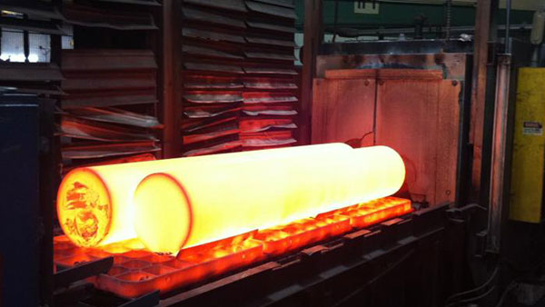
Failure Analysis & Material Investigation
Resource Secondment
Corrosion Test & Investigation
SEM/EDS
Microstructure Analysis
Heat Treatment Consultancy
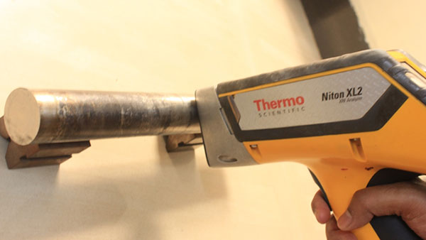
PMI Test
Training
Mechanical Testing
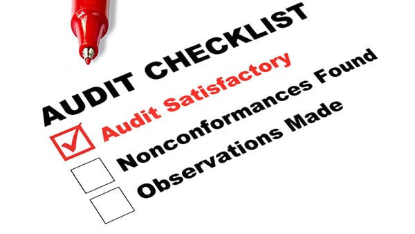
Supplier Evaluation Audits
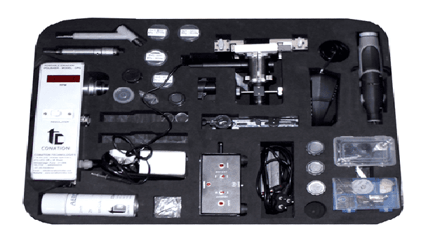
In-Situ Metallography and Replica Extraction
Popular Search: SEM Analysis Lab in Chennai | Sem Testing Near me| EDS Lab | MTS-India