Using Scanning Electron Microscopy Testing Lab to Identify Metal composition
To understand the topography and composition of an element Scanning Electron Microscopy Testing Lab uses a concentrated electron beam on the face of the product to create an image.
These electrons then interact with the sample and produce distinguished signals which provide the information regarding the element.
Why one prefers the use of electron instead of light in a microscope?
When sufficient light is given, a human eye can distinguish two points that are 0.2mm apart without any additional lens. This distance is known as the resolution of the eye or the revolving power. A lens or an assembly of the lens can amplify the distance and enable the eye to see the points closely.
A modern light microscope will provide maximum amplification of 1000X. The number of lenses used, and the wavelength of the length used for illumination are some of the reasons for the limitation of the microscope’s resolving power.
The wavelength of the light usually between 400 to 700 nanometres. The average wavelength is considered 550mm, which results in a theoretical limit of resolution, i.e., no visibility of the microscope in a white light about 200-250nm.
An electron microscope was developed when the wavelength becomes the limiting factor in a light microscope. Since electrons have much shorter wavelengths, it enables better resolution.
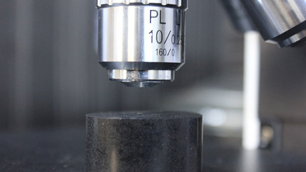
Comparing an optical microscope to a scanning electron microscope
Due to new technology, the elements are being downsized in terms of their dimensions, and they can no longer be portrayed with the help of light microscopy. For instance, for analysis of the integrity of a nanofiber layer for filtration, electron microscopy will prove to be far better than optical microscopy.
How does Scanning Electron Microscopy Testing Lab work?
The main components of scanning electron microscopy are the source of electrons, the column down through which the electrons travel with electromagnetic lenses, electron detector, sample chamber, and the computer that will display the images.
The electrons are produced on top of the column and then accelerated down and passed through the combination of lenses and holes to generate a concentrating beam that will hit the surface of the sample of the element. The sample will be mounted on a stage within the chamber area.
Unless the microscope is designed to work in a low vacuum, both the chamber and column are evacuated by using a combination of pumps. The design of the microscope will decide the level of vacuum.
With the help of the scan coils, the position of the electron beam is controlled, which is situated above the objective lens. These coils will allow the beams to scan the surface of the sample.
As the name of the microscope suggests, the beam scanning the surface of the sample will enable the information around a defined area on the piece that will be collected. Based on the electron and elements of the surface interaction, distinguish signals will be produced.
With the help of the detectors, these signals are detected, and the computer will note down the information and display it for viewing.
Sample Electron Interaction
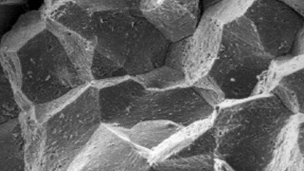
The scanning electron microscopy will produce the images by scanning the sample of the product with a high-energy beam of electrons. As the electrons collaborate with the sample, they will generate secondary electrons, characteristic X-rays, and backscattered electrons.
These signals are then collected by more than one detector present in the chamber, and they form the images which are displayed by the computer screen.
When the concentrated beam of electron hits the surface of the sample, it will penetrate the depth of the sample by a few microns and depending on the acceleration voltage of the beam and the density of the element face.
Many signals like X-rays and secondary electrons are produced, resulting from the collaboration of the beam with the face of the sample.
Multiple factors are responsible for the maximum resolution obtained in a scanning electron microscopy testing lab. For instance, the electron spot size and the interaction level of the electron beam is with the surface of the sample.
While microscopy can provide atomic resolution, some of the microscopes can achieve a resolution below 1nm.
Generally, a modern full-sized scanning microscopy will generate a resolution between 1nm-20nm, whereas the desktop system will be able to provide a resolution of around 20nm and more.
Analysis application
The signals generated through electron microscopy will provide a two-dimensional image and reveal information about the sample. This will include the external morphology, which is the texture of the sample, the chemical composition; by using additional features, it will also provide information regarding the orientation of the sample.
With additional features of energy dispersive X-ray, the microscopy will determine the elements that are in or on the surface of the sample with qualitative information.
It will also measure the elemental composition for semi-numerical results, identifying the foreign substance that is not organic in nature and is a coating on the metal.