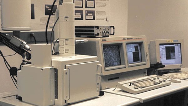
Scanning electron microscopy (SEM) analyzes the surface of materials. SEM measures and evaluates surface pitting, failure analysis, characterization of dust, deposits, contaminants, particles, filter residues, and other applications.
MTS Metallurgists analyse the surface of solid objects, producing higher resolution images than optical microscopy.
Micro structural characterization includes the analysis of materials, polymers, films, coatings, geological and mineral core samples, pharmaceuticals, raw materials, metals, plastics, ceramics, glass, food, dust, contaminants, unknowns and other products.
MTS India offers state-of-the-art SEM and EDS Analysis Lab services, providing in-depth microstructural and elemental analysis of a wide range of materials. Using Scanning Electron Microscopy (SEM) combined with Energy Dispersive Spectroscopy (EDS), we help industries investigate surface features, contaminants, coatings, and compositional anomalies with high accuracy and resolution.
Whether you’re dealing with component failure, process contamination, or material verification, our SEM and EDS capabilities offer powerful insights at the microscopic and elemental level. From metals and polymers to pharmaceuticals and geological samples, MTS India is your trusted partner for precision material characterization.
SEM (Scanning Electron Microscopy) is an advanced imaging technique that uses a focused beam of electrons to scan a sample surface. It provides highly magnified, three-dimensional images that reveal fine details of microstructure, morphology, and surface features.
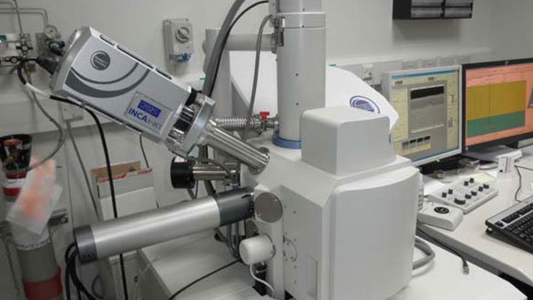
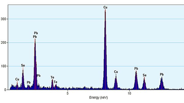
EDS (Energy Dispersive Spectroscopy) is an elemental analysis technique integrated with SEM. It identifies and quantifies the elemental composition of the sample surface or a specific feature in the SEM image.
Together, our SEM and EDS Analysis Lab allows for comprehensive visual and chemical analysis — a critical advantage in materials science, failure analysis, quality control, and contamination investigations.
At MTS India, we combine high-resolution imaging with precise elemental detection to deliver:
Our SEM instruments deliver magnifications up to 300,000x, far exceeding what traditional optical microscopy can achieve.
With EDS, we can pinpoint and analyze the presence of elements in specific areas, revealing composition, contamination, or inclusion details.
Our SEM and EDS Analysis Lab supports a wide variety of sample types — metals, polymers, ceramics, composites, films, dust particles, and more.
We offer quick turnaround times with high-quality micrographs, element spectra, and expert interpretation tailored to your industry needs.
MTS India’s SEM and EDS Analysis Lab plays a vital role in several industrial and research applications:
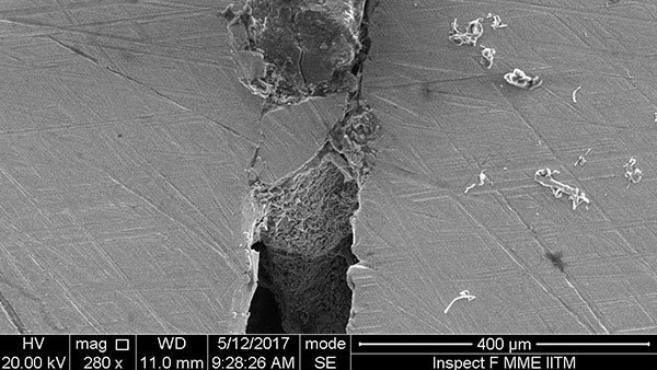
Identify root causes of material failure such as cracking, fatigue, pitting, wear, or corrosion. SEM provides visual evidence while EDS confirms elemental composition in the affected zone.
Examine surface coatings, welds, thin films, and polished cross-sections to assess uniformity, grain size, phase distribution, or surface treatment effects.
Analyze unknown particles, residues, or inclusions found in manufacturing lines, cleanrooms, pharmaceutical batches, or filter systems. Our SEM and EDS analysis helps determine source and composition.
Confirm that your materials match required specifications. SEM imaging and EDS testing reveal structural and compositional irregularities before they become operational problems.
Visualize and quantify localized corrosion (pitting, intergranular attack) and study corrosion product composition to trace causes.
Examine the quality, adhesion, and thickness of coatings and multilayered materials. Determine failure modes such as delamination or voids.
Our SEM and EDS Analysis Lab supports a wide range of industries including:
Our lab is equipped and staffed to handle your unique challenges with technical precision and industry-specific expertise.
MTS India’s SEM and EDS Analysis Lab is equipped to examine:
Each material requires tailored preparation and imaging techniques, which our metallurgists and analysts expertly handle.
You can submit solid samples, cross-sections, powders, or filters. Our team can guide you on ideal sizes and preparation if needed.
Depending on the sample type, we mount, polish, and coat it (if non-conductive) to prepare it for SEM examination.
The sample is placed in the SEM chamber where it is scanned under high vacuum using an electron beam. We capture high-resolution images of the surface and sub-surface features.
Elemental analysis is conducted on selected zones of interest. We generate element maps and line scans to visualize and quantify the composition.
Our experts compile a detailed report including SEM micrographs, EDS spectra, element maps, and interpretive commentary. We also provide failure insights or recommendations if required.
MTS India is one of the leading providers of SEM and EDS Analysis Lab services in the country. Our strengths include:
✅ Cutting-edge instrumentation with high magnification and accuracy
✅ Experienced metallurgists and material scientists
✅ Support for a wide range of industries and sample types
✅ Rapid turnaround and responsive customer support
✅ Customized reporting with actionable insights
Whether you’re in R&D, quality assurance, or forensic investigation, MTS India is your trusted partner for microstructural and elemental analysis.
SEM can accommodate very small samples — as little as 1 mm in size. However, sample preparation may vary based on the material.
Yes, but detection of lighter elements (like carbon, nitrogen, and oxygen) can be limited depending on the detector used. We advise clients accordingly.
SEM is minimally destructive. Non-conductive materials may require a thin coating (like gold or carbon), but bulk integrity is preserved.
Standard SEM and EDS analysis can be completed within 2–5 working days, depending on sample type and scope of work.
Looking for detailed surface and elemental analysis with unmatched clarity? Trust MTS India’s SEM and EDS Analysis Lab to provide the insights you need for product improvement, failure prevention, and material innovation.
📞 Call us at +91 98417 07777
📧 Email: info@mts-india.in
🌐 Website: https://mts-india.in/
Unlock the power of electron microscopy and take your material analysis to the next level with MTS India.
Popular Search : SEM Analysis Lab in Chennai | Sem Testing Near me| EDS Lab | MTS-India

We are a unique laboratory in India focusing on Failure Analysis and one of the few finest NABL accredited Metallurgical laboratories in the country.